
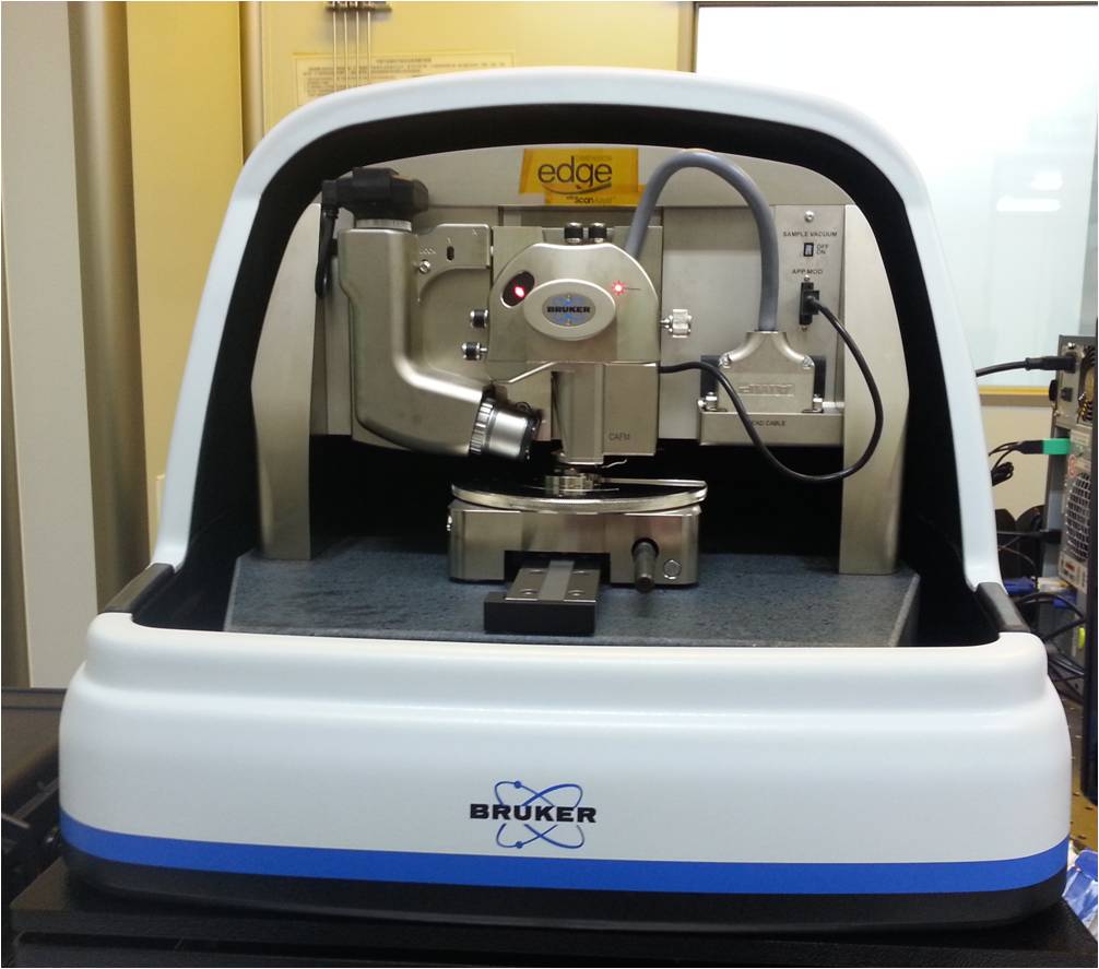
INTRODUCTION:
Fast Scanning Probe Microscopy with Nanoscratch Function is a test platform consists of the brought up AFM and a self-designed test part. The atomic force microscopy (AFM) can perform the imaging of high precise surface morphology, static electrical force EFM and magnetic force MFM, while the self-designed part can perform the nanoscratch test and friction force test with micro-Newton level load, and the surface contact resistivity test. The aforementioned nanosurface tests on its mechanical, electrical, magnetical, and morphological properties are the basic ways to perform the nanosurface science and engineering research.
SPECIFICATION:
Piezoelectric motion platform
XYZ Closed-Loop Application Module-ready SPM Scan Head with a nominal range of 90-micron x 90-micron and vertical range of 10-microns
Low-noise Closed-Loop: 0.5 nm in X, Y-axis and 0.2 nm in Z-axis
Dimension Edge NanoDrive controller (X, Y-axis): 150 mm×150 mm
Optical system: 5 million digital camera with visible area from 180 mm to 1465 mm
Surface morphology test : contact, tapping, peak force modes, scanning tip curvature radius 4-10 nm
Magnetic force (MFM) test : Tapping mode with lift height 20-100 nm, magnetic hysteresis phase shift accuracy 5×10⁻³ °
Electrostatic force (EFM) test: loading voltage10~+10 V (low) /-220~+220 V (high), electrostatic force resolution 0.3 mV
Nanoscratch test: Scratching load 100uN-10 mN, Scratching speed 6 mm/s, Scratching length 1-150 um
Friction force test: Friction force resolution 100 mN, sliding velocity 0.1 mm/s -10 mm/s
Surface contact electric resistance: accuracy from kW to MW level